Sensor Selection

Sensor Size

Pixel Size

Pixel Density
The selection of the appropriate sensor for your purposes in defined primarily by your intended use. FLI cameras are available with sensors optimized for every corner of the scientific world. Variables such as sensor type, size, and shape, alongside pixel size and density will help define which sensor is appropriate for its intended use.
A list of all available sensors alongside information regarding each sensors qualities is available on this chart:
Sensors Supported in FLI Cameras
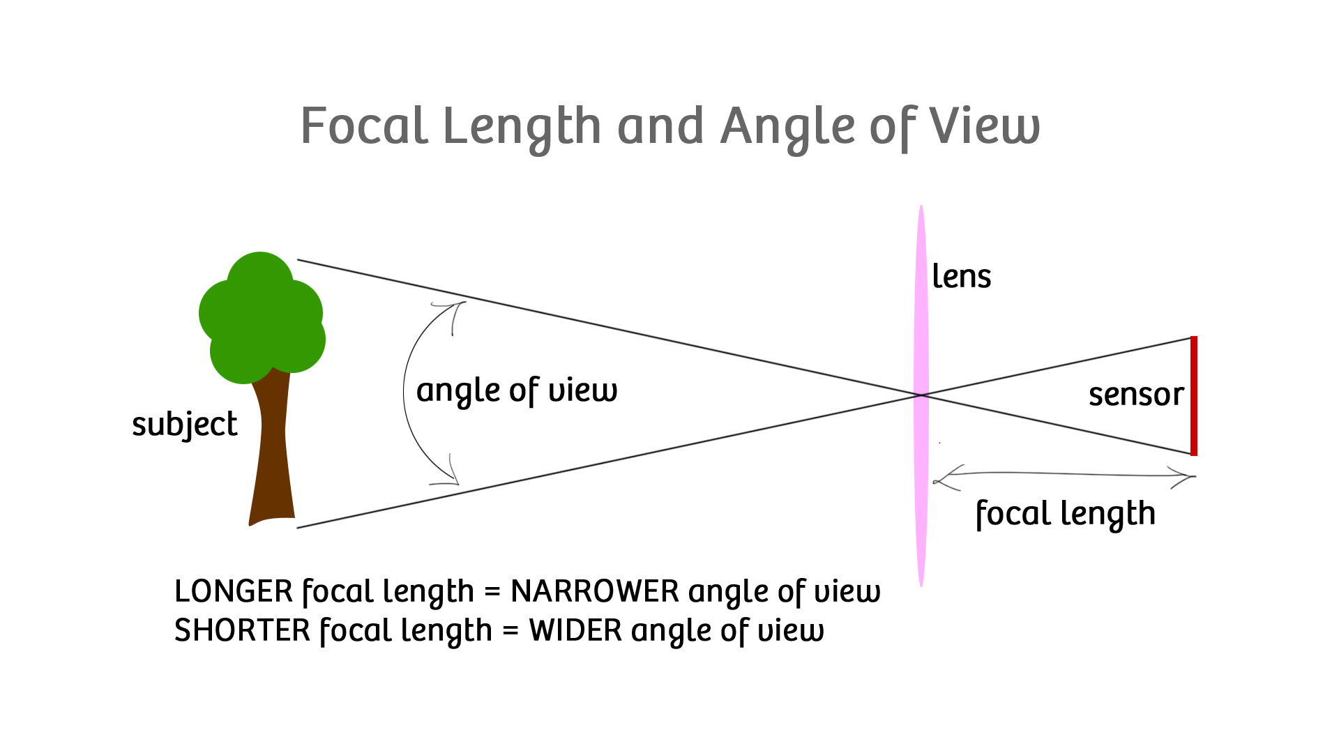
Sensor size influences the field of view of the image. A sensor with a large area can capture a larger area of light, resulting in a larger field of view. A sensor with a small area cannot capture the same area of light, resulting in a narrower field of view. Each sensors area, in mm2, is displayed in the chart referenced above.
Pixel size is very important to quality imaging. A pixel with a large area will collect more light, however it will result in a decreased resolution, as the pixels precision is lost when it collects light over a large area. A pixel with a smaller area will collect less light, but it will hold more precision by better identifying the location of where photons impacted the sensor. On the chart referenced above, pixel size is shown as a measure of microns, another name for which is micrometers.
As displayed in Figure 4, the wide pixel bucket has capacity to not only store more light information, but collect light from a greater area.
The decision of what size a sensor's pixels needs to be is often concluded with a balance between resolution and sensitivity. A system intended for low light situations should prefer larger pixels, while a system intended for well lit scenes should prefer smaller pixels.
High density pixel arrangements collect less light with more precision, while low density pixel arrangements collect more light with less precision. On the chart referenced above, there is no given measure of pixel density; however, you can get a good idea of how each sensor compares by taking the number of pixels and dividing it by the sensor area. For example, the KAF-4301 has a pixel density of approximately 1700pixels/mm2, while the KAF-50100 has a pixel density of approximately 28,000pixels/mm2. The KAF-50100 is clearly much more dense than the KAF-4301 because it has almost 16 times more pixels the amount of pixels per mm2.
Pixel density goes hand in hand with pixel size. As pixel density increases, the size of the pixels must decrease. High density sensors have a greater number of pixels, and thus have greater precision when identifying where light came from, producing higher resolution images. Low density sensors, however, include larger pixels more capable of collecting light when there is not a lot of light in the scene.
Figure 4: Effect of Pixel Size
Image Credit: Jon Minnick, cloudbreakoptics.com
Image Credit: Jon Minnick, cloudbreakoptics.com
Figure 5: Effect of Pixel Density
Image Credit: Jon Minnick, cloudbreakoptics.com
Image Credit: Jon Minnick, cloudbreakoptics.com

Sensor Type

Sensor Illumination

Quantum Efficiency
There are two primary sensor types to chose from: CCD and sCMOS. On the chart referenced above, any GPixel sensor is a sCMOS sensor, and any of the other sensors are CCD.
CCD sensors provide low dark current images at the cost of higher frame rate availablility. These sensors are ideal for long exposure imaging. CCD sensors are discussed further here.
sCMOS sensors provide images with very low noise, significantly higher frame rates, and a large field of view. sCMOS sensors are ideal for imaging requiring quick image capture and low noise. sCMOS sensors are discussed further here.
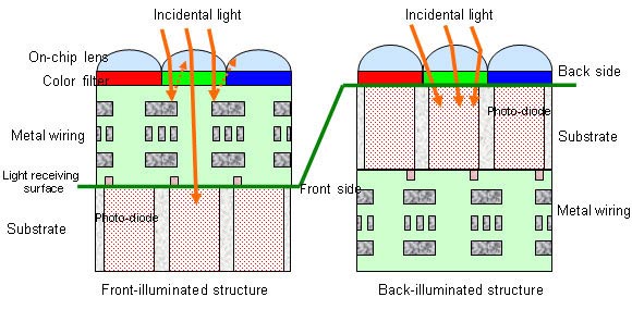
Two options exist with sensor illumination, backside and frontside. The root of this option sprouts from a pixels architecture. Figure 6 shows how front illuminated sensors require light to first pass through a layer of circuitry on the front side of the photodiode. Inversely, back illuminated sensors place the circuitry on the backside of the photodiode. Back illuminated sensors require a significantly more challenging procedure to produce. Thus, black-illuminated sensors are more expensive that front illuminated sensors.
Quantum efficiency (QE) is provided as a percentage and is a measure of efficiency a sensor can measure incident photons. We know light to be composed of photons, objects which we can then measure with photodiodes. With a sensor capable of 100% QE, the photodiodes of the sensor would translate one incident photon into one measurable electron. As QE decreased towards 90%, 50%, etc, the amount of photons recorded by the sensor decreases, subsequently resulting in decreased sensitivity to light.
High QE sensors capture the most light, and thus are more sensitive imaging devices. Devices with low QE may suffer from dark images, and will not operate optimally in low light situations.
The image to the right shows an example of a pixel with decreased QE (on the right). As light enters the pixel well, some is reflected, some is absorbed, and some gets to the sensing area. The more in the way of the lights path, the lower the QE is due to less light being read.
The pixel to the right would be an example of a front illuminated sensor, with various objects blocking the lights path.
QE is not shown on the chart referenced above, however, a simple internet search of the sensor ID, example: KAF-50100, will return the sensor specifications from the manufacturer and will include the sensors quantum efficiency.

Sensor Shape
The FLI cameras come with two available shapes. While the shapes are not explicitly stated on the chart referenced above, one can deduce from the array size (X and Y) that some sensors are square and nearly square, and others are much wider than they are tall.
The most common is square and rectangular with similar height and width dimensions (Figure 2). These sensors are applicable for nearly every use for a camera.
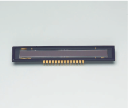
The second available option is the Hamamatsu horizontally stretched sensors, which are significantly wider than they are tall (Figure 3). These sensors are well designed for applications such as spectrophotometry, but are not well designed for most applications.

Figure 2: GSense400
Image Credit: GPixel, gpixel.com
Image Credit: GPixel, gpixel.com
Figure 3: S9979
Image Credit: Hamamatsu, hamamatsu.com
Image Credit: Hamamatsu, hamamatsu.com

Finger Lakes Instrumentation
1250 Rochester St.
Lima, New York 14485
1250 Rochester St.
Lima, New York 14485
Phone: 585-624-3760
Email: sales@flicamera.com
Web: https://flicamera.com
Email: sales@flicamera.com
Web: https://flicamera.com
©2024 Finger Lakes Instrumentation

Figure 1: Sensor Size and Field of View
Image Credit: Jack Hollingsworth, snapsnapsnap.photos
Image Credit: Jack Hollingsworth, snapsnapsnap.photos

Figure 6: Pixel Illumination
Image Credit: Sony, Sony.net
Image Credit: Sony, Sony.net
Figure 7: Quantum Efficiency Example
Image Credit: Jon Minnick, cloudbreakoptics.com
Image Credit: Jon Minnick, cloudbreakoptics.com
The chart referenced above shows front illuminated sensors with a red font, and the back illuminated sensors with a blue font. Sensors shown in neither a red nor blue font are interline transfer CCD sensors, which are discussed in further detail on the CCD Sensors page.
interline transfer sensors are a type of CCD sensor that do not provide a choice between front/back illuminated, thus earn their own category. Interline transfer sensors are less sensitive to light due to their architectures, however, they avoid smear and are capable of higher image capturing rates than other CCD architectures.
Back illuminated sensors allow more light into the photodiode, because less light is blocked, reflected, or absorbed by the circuitry in a frontside illuminated sensor. With this increased light, the low-light capabilities of the sensor are enhanced, and digital noise is reduced.
Back illuminated sensors are ideal for low light imaging, due to its ability to capture more light.
Front illuminated sensors are ideal for imaging devices not expected to be used in low light situations.
Interline transfer sensors are ideal for high rates of frame captures, but not very low light situations.
If one can imagine the size of the sensor in the Figure 1 modulating between larger and smaller, with the lines drawn from its edges intersecting at the same location, one may note that the angle of view increases as sensor size increases, thus capturing a larger portion of the scene.
